


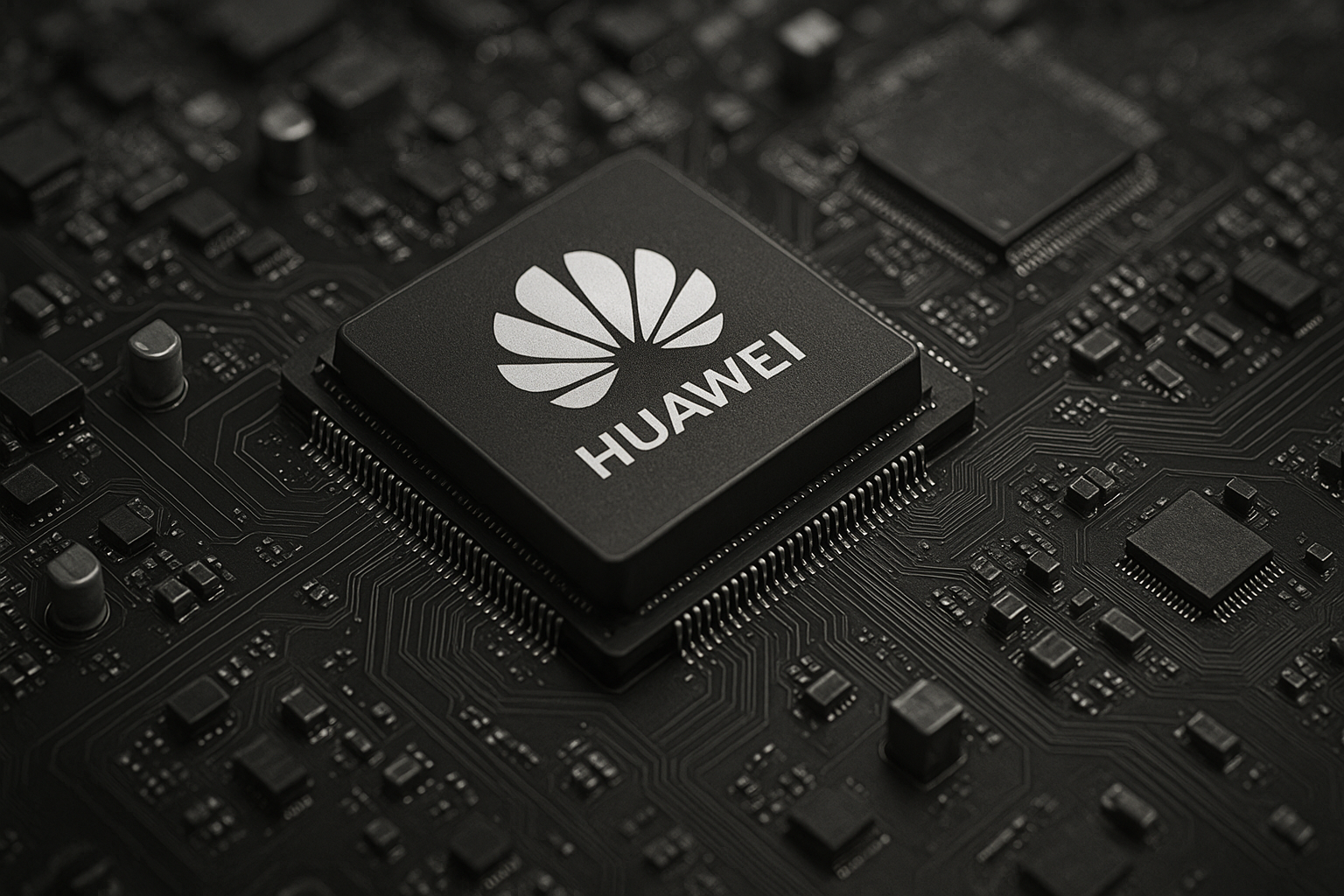
Huawei’s Cutting-Edge Tech Advances Amidst Sanctions
Huawei Technologies is making strides in advanced lithographic technologies, potentially surpassing expectations with its in-house developed chips. Despite sanctions, these advancements could position Huawei to rival global tech leaders in producing cutting-edge semiconductor components.
Progress in Chip Manufacturing
The HiSilicon Kirin X90 processors, recently introduced, stem from the enhanced 7-nanometer (nm) process by SMIC, contrary to the anticipated 5-nm standard. Leveraging improved chiplet packaging, Huawei has managed to boost transistor density, although the yield rate remains below 50%, leading to high production costs.
Independent Production Capabilities
Huawei has developed production lines independent of foreign lithographic equipment, using Shanghai Micro Electronics’ SSA800 series for chip design exposure. By employing multiple passes and templates, Huawei achieves the necessary physical parameters for its chips. Silicon wafer etching is executed with AMEC’s equipment, capable of handling 5-nm processes, while Naura Technology provides precise testing equipment.
This ecosystem not only aids Huawei but also empowers other Chinese chipmakers to progress in lithography, despite ongoing U.S., Japanese, and Dutch sanctions.
3-nm Technology on the Horizon
With plans to adopt planar structures and gate-all-around (GAA) transistors, Huawei is gearing up to implement a 3-nm process next year. An innovative alternative utilizing carbon nanotubes has passed lab tests and is under trial at SMIC’s facilities, signaling potential technological breakthroughs.
As Huawei navigates these advancements, its efforts could reshape the competitive landscape, challenging existing international tech leaders.