

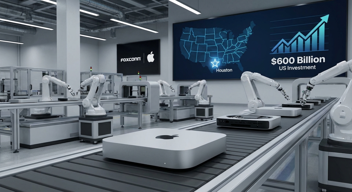


According to the Korea Economic Daily, Samsung plans to initiate the trial operation of EUV equipment at its Taylor Plant 1 in Texas as early as March this year. This stage marks the preparation for mass production of chips using the advanced 2-nm process technology with GAA (Gate-All-Around) transistors on American soil.
The factory in Texas will serve as a platform for fine-tuning key technological processes-installation, etching, and deposition using extreme ultraviolet lithography. The full-scale launch of series production is expected in the second half of 2026. While it is not yet specified if Exynos 2600 processors will be produced there, it is known that the plant will become the production base for Tesla’s AI chips. These include the AI5 and AI6 SoCs, which Samsung will manufacture under a contract signed last year valued at $16.5 billion. Approximately 7,000 workers have been deployed to expedite the plant’s activation. Upon completion of construction, up to 1,000 employees will be housed in a six-story production complex. The company is also preparing to obtain a temporary operational permit necessary to confirm the facility’s compliance with fire safety and other regulations.
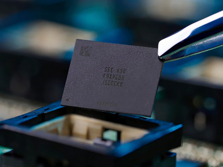
The Texas site, spanning 4.85 million square meters, exceeds the largest Korean Samsung factories in Pyeongtaek and Hwaseong combined. A key element of Samsung’s strategy remains the purchase of EUV machines from ASML-each costing around 500 billion won ($339 million). These investments are crucial as the yield of viable products manufactured using the 2-nm process at this stage is estimated at 50%. Improving these figures is necessary to achieve profitability for the semiconductor division by 2027, especially against the backdrop of losses of $680 million recorded in the third and fourth quarters of 2025.
In the future, Samsung plans to build up to ten factories on the Texas site. Initially, the enterprise was focused on the 4-nm process, but TSMC’s refusal to transfer advanced technologies to the US opened a strategic window of opportunity for Samsung. The initial goal is to produce up to 50,000 silicon wafers.