


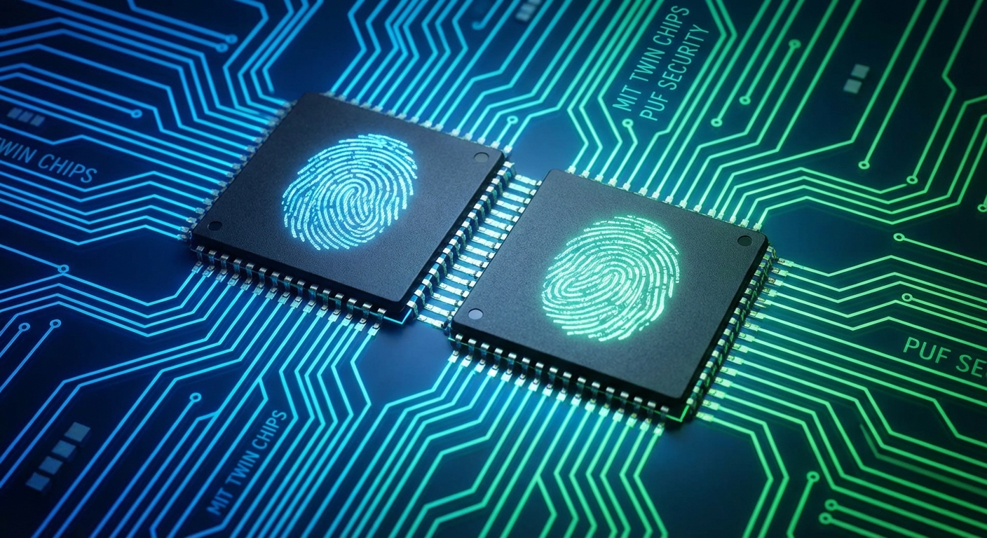
Every CMOS chip is unique due to microscopic manufacturing variations, much like a human fingerprint. These differences create a Physical Unclonable Function (PUF), which is used to authenticate devices. However, traditional schemes require storing data on external servers, creating vulnerabilities and complicating security. Engineers at the Massachusetts Institute of Technology (MIT) have proposed a fundamentally new approach: they have learned to create “twin fingerprints” on a pair of chips during the manufacturing stage.
The Flaw in Traditional Authentication
For years, PUF technology has been a cornerstone of hardware security. The unique response of a chip to a specific input (a challenge) serves as its digital signature. To verify a device, a server sends a challenge and checks if the chip’s response matches the one stored in its database. The problem lies with this database. It represents a single point of failure; if compromised, an attacker could create clones or spoof legitimate devices. This server-dependent model is a significant bottleneck for creating truly secure, decentralized systems, especially for low-power devices.
A Breakthrough in Chip Twinning
The MIT method, presented at the IEEE International Solid-State Circuits Conference, revolutionizes this process by creating a shared secret directly between two chips. To achieve this, pairs of transistors are formed along the edge of two future microchips. A controlled breakdown is then induced using a low-cost LED, which essentially applies a high voltage to the transistors. Due to random structural variations, each pair of transistors gets a unique but matching fingerprint. After the chips are separated, their PUF keys match by more than 98%-a rate sufficient for reliable mutual authentication.
The main advantage is that the secret data never leaves the chip. Two devices can directly confirm each other’s authenticity without contacting a server or transmitting keys over a network. This method is compatible with standard CMOS manufacturing, requires no expensive materials, and is suitable for mass adoption, including in energy-efficient medical sensors and IoT devices.
The Future of Hardware-Level Trust
This innovation moves beyond simple authentication and into the realm of creating trusted hardware pairs from the moment of creation. The authors note that in the future, the technology will allow for the creation of secure device pairs-for example, a smart pill and a wearable health monitoring patch that can authenticate each other without intermediaries. This opens new horizons for hardware security and protected data transmission. According to MIT provost Anantha Chandrakasan, this approach delivers both energy efficiency and robust security, which are crucial for real-world deployment in connected medical devices and smart sensors. By leveraging the fundamental physics of chip manufacturing, this approach could become the foundation for new security standards, enabling a future of truly independent and secure interconnected devices.