


Intel, through its branch Intel Foundry, has announced the installation of the world’s most advanced machine for EUV lithography at its factory – the TWINSCAN EXE:5200B High-NA EUV scanner from ASML. This machine is crucial for Intel’s 14A process, on which the company is now placing significant bets. The use of this High-NA EUV lithography (extreme ultraviolet lithography with high numerical aperture) marks the first industry transition from low-NA to high-NA lithography.
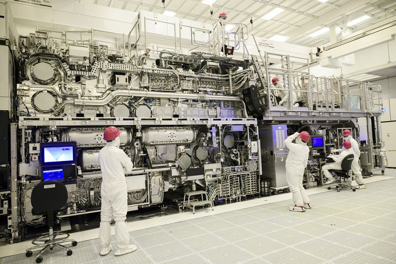
In collaboration with ASML, the processor giant has already completed acceptance testing. The TWINSCAN EXE:5200B is the second version of the High-NA EUV scanner from ASML, following the TWINSCAN EXE:5000, which Intel initially used for its trial runs of the 14A technology. The new machine offers a throughput of 175 wafers per hour under standard conditions, but Intel aims to increase this figure to more than 200 wafers per hour. The installation also enhances alignment accuracy, providing alignment of individual lithographic layers to a precision of 0.7 nanometers. Serial production using the new process is planned to begin in 2027.
Intel emphasizes that this process stands out because the company’s partners are involved in its development from the outset, which will subsequently allow for faster and easier creation of chips that are optimally suited to customer needs.
The move to high-NA technology is anticipated to enable semiconductor manufacturers, especially Intel, to lower costs and improve power efficiency, a critical step as the industry races toward smaller nodes and more powerful chips.
Despite these technological leaps, Intel faces competitive pressure from other major semiconductor players like Taiwan Semiconductor Manufacturing Company (TSMC) and Samsung, who are similarly advancing their lithographic technologies.