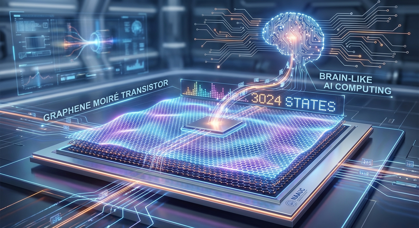
Engineers from Nanjing University of Aeronautics and Astronautics in China have developed a groundbreaking ferroelectric transistor just a few atoms thick, signaling a potential revolution in memory and neuromorphic computing. The device leverages layered 2D materials-graphene and hexagonal boron nitride (hBN)-which, when stacked, create a unique moiré pattern. This structure’s main feature is its ability to store 3,024 different polarization states, a figure that is two orders of magnitude greater than previous analogs. This breakthrough is achieved through the precise control of electrical impulses that cause the atomic layers to slide relative to each other.

The Magic of Moiré Engineering
The core of this innovation lies in the physics of moiré superlattices. When two-dimensional crystalline layers with slightly different lattice structures, like graphene and hBN, are overlaid, they produce a larger, repeating interference pattern-much like the visual effect seen when looking through two overlapping fences. This moiré pattern creates a new periodic potential that dramatically alters the electronic properties of the material. In this transistor, the sliding ferroelectricity mechanism allows for the creation of a vast number of stable, non-volatile states, each corresponding to a specific alignment of the layers.
A Quantum Leap in Data Density and Performance
The ability to hold 3,024 distinct states in a single transistor represents a monumental leap in data density. For context, modern high-density NAND flash memory technologies like Quad-Level Cell (QLC) store 16 states (4 bits) per cell. The new device surpasses this by an exponential margin, opening the door for ultra-dense memory solutions. The transistor has demonstrated high stability, maintaining its programmed states for over 100,000 seconds (more than 27 hours). Furthermore, it has proven its practical application in AI tasks, achieving an impressive 93% accuracy in image recognition tests. The device operates effectively at both room and elevated temperatures, and its relatively simple structure is a key advantage for future scalability.
Powering the Next Generation of AI
Such multi-state transistors are ideal building blocks for neuromorphic chips, which are designed to mimic the structure and efficiency of the human brain. A major challenge in current computing, known as the von Neumann bottleneck, is the energy and time wasted moving data between separate processing and memory units. Neuromorphic systems perform in-memory computing, where data processing occurs in the same place it is stored. The vast number of states in this new transistor allows it to function as a highly nuanced artificial synapse, capable of storing complex weights and patterns far more efficiently than binary systems. This could lead to significantly more powerful and energy-efficient AI for applications ranging from large model inference to edge intelligence and wearable devices.
The Road Ahead: From Lab to Fabrication
While this breakthrough is significant, the primary challenge lies in transitioning from a laboratory prototype to mass production. The team plans to focus on increasing the device’s response speed and developing scalable manufacturing processes. The field of advanced memory is highly competitive, with other promising technologies like Hafnium Oxide-based FeFETs and MRAM also under intense development. However, if the scaling and speed challenges can be overcome, this moiré-based ferroelectric transistor could become a foundational technology for the future of high-density, low-power electronics.


