

Amid a booming market for AI chips, Samsung Electronics’ Device Solutions (DS) division is undertaking a strategic optimization of its business, aiming to push its operating margin above an ambitious 50%. The core of this new strategy involves reorienting production and sales to focus on high-profitability products, primarily its most advanced DRAM memory and next-generation 2nm foundry services. This move signals Samsung’s intent to capitalize on the current semiconductor supercycle and solidify its leadership in both the memory and logic chip sectors.
The High-Margin Memory Gambit
For Samsung, the most immediate path to higher margins lies in its DRAM business, which is currently a major cash cow with profit margins already hitting 50% due to soaring demand. The company is intensely focused on its sixth-generation 10nm-class (1c) DRAM process. A key challenge has been the manufacturing yield rate; while the initial text mentioned a 60% yield, more recent reports from mid-2025 indicate significant progress, with yields now reaching between 50% and 70%. This is a substantial improvement from earlier figures but still short of the 80-90% threshold considered ideal for full-scale, cost-effective mass production.
Mastering the 1c process is critical as it forms the foundation for Samsung’s next-generation HBM4 (High Bandwidth Memory). The AI boom has turned HBM into a fiercely competitive and lucrative market, and Samsung is in a tight race with rivals SK Hynix and Micron to supply major customers like NVIDIA. By boldly using the more advanced 1c process for HBM4, Samsung is taking a calculated risk that could yield significant technological and market share advantages if successful.
The Foundry Frontier: Scaling at 2nm
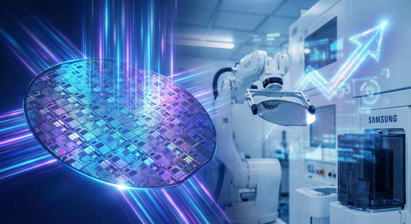
The second pillar of Samsung’s strategy is its foundry business, where it aims to capture a larger share of the advanced chip manufacturing market. The company is targeting a remarkable 130% increase in orders for its 2nm Gate-All-Around (GAA) process this year. This aggressive goal is backed by tangible progress in its technology. After early struggles, Samsung has improved its 2nm process yields to a much more stable 55-60%, making it a more attractive option for major clients.
This technological maturation has already helped Samsung secure significant orders, including a reported multi-billion dollar deal with Tesla. With the market leader TSMC facing overwhelming demand for its advanced nodes, Samsung is positioning itself as a viable high-volume alternative, potentially attracting other major clients like AMD. While the foundry business has been a financial drag, this push into 2nm production is expected to steer it toward profitability by 2027.
A Two-Pronged Strategy for Dominance
Samsung’s dual focus on memory and foundry is a synergistic strategy. The record-breaking profits generated by the memory division, which recently posted its highest-ever quarterly revenue, provide the massive capital required to fund the research and expansion of its cutting-edge foundry operations. The DS division’s overall operating profit has surged, with analysts expecting the chip segment to post record results, providing the financial muscle to challenge competitors on multiple fronts.
Future Outlook: High Stakes in the Chip War
Samsung’s goal of a 50% operating margin is more than a financial target; it is a declaration of its ambition to dominate the next generation of semiconductors. The AI-driven demand has created a golden era for memory manufacturers, and Samsung is leveraging this boom to fuel its long-term foundry aspirations. However, the path is fraught with challenges. The company faces intense competition from an entrenched SK Hynix in the HBM market and the formidable task of closing the market share gap with TSMC. Successfully executing this two-pronged strategy could cement Samsung’s position as an unparalleled leader in the global semiconductor industry for years to come.